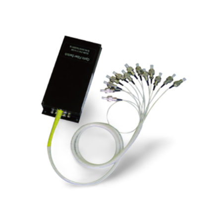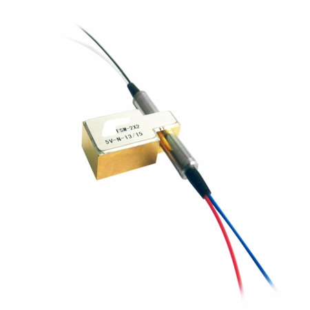
Fiber Optic 1XN Switch with connector for Network Solutions Manufacture in China
Brand Kalinton
Product origin China
Delivery time 7-15 days
Supply capacity 50000pcs
Product Name: Fiber Optic 1XN Switch with connector for Network Solutions Manufacture in China
Specifications
ParametersUnitJXT-FSW-1×N
Insertion LossdB1 < N ≤ 4545 < N ≤ 8888 < N ≤ 128
Typ: 0.8 Max: 1.0Typ: 1.2 Max: 1.5Typ: 1.5 Max: 1.8
Wavelength Rangenm850±40 / 1300±401260 ~ 1650
Test Wavelengthnm850 / 13001310 / 1550
Return LossdBMM ≥ 30 SM ≥ 50
CrosstalkdB≥ 55
PDLdB≤ 0.05
WDLdB≤ 0.25
TDLdB≤ 0.25
RepeatabilitydB≤ ±0.05
DurabilityCycles≥ 10 Million
Switching Timems≤ 10 (Sequence switch time of adjacent channel)
Optical PowermW≤500
Operating Temperature℃-20 ~ +70
Storage Temperature℃-40 ~ +85
Relative Humidity%5 ~ 95
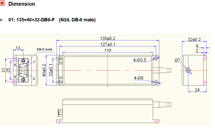
Dimension mm:135×40×32 (N≤4) 135×64×32 (N≤12)184×78×36 (N≤16)
184×78×66 (N≤45)184×156×66 (N≤88)184×220×66 (N≤128)
140×77.5×32 (N≤16)140×77.5×64 (N≤32)
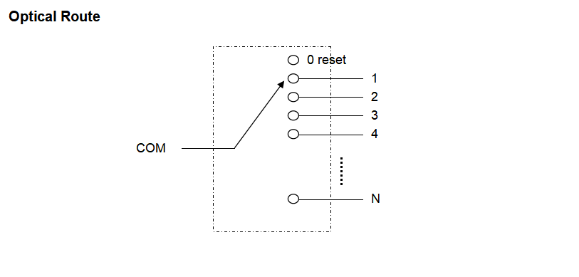
1×N Optical switch is a kind of functional component, with the ability of switching optical route. In optical fiber transmission system, it is used for multi-channel fiber monitoring, multi light source/ detector selection, and optical fiber path protection etc. Besides, it is also used in optical fiber test system for optical fiber and its component test, outdoor cable test and multi-spot optical sensors monitoring system.
Product Name: Fiber Optic 1XN Switch with connector for Network Solutions Manufacture in China
Features
·More Than 128 Channels
·Low Loss and High Reliability
·Parallel Interface (TTL)
·Modularized Design
·Epoxy-free on Optical Path
Applications
·Ring Network
·Remote Monitoring in Optical Network
·Testing of Fiber, Optical Component
Specifications
Parameters | Unit | JXT-FSW-1×N | |||
Insertion Loss | dB | 1 < N ≤ 45 | 45 < N ≤ 88 | 88 < N ≤ 128 | |
Typ: 0.8 Max: 1.0 | Typ: 1.2 Max: 1.5 | Typ: 1.5 Max: 1.8 | |||
Wavelength Range | nm | 850±40 / 1300±40 | 1260 ~ 1650 | ||
Test Wavelength | nm | 850 / 1300 | 1310 / 1550 | ||
Return Loss | dB | MM ≥ 30 SM ≥ 50 | |||
Crosstalk | dB | ≥ 55 | |||
PDL | dB | ≤ 0.05 | |||
WDL | dB | ≤ 0.25 | |||
TDL | dB | ≤ 0.25 | |||
Repeatability | dB | ≤ ±0.05 | |||
Durability | Cycles | ≥ 10 Million | |||
Switching Time | ms | ≤ 10 (Sequence switch time of adjacent channel) | |||
Optical Power | mW | ≤500 | |||
Operating Temperature | ℃ | -20 ~ +70 | |||
Storage Temperature | ℃ | -40 ~ +85 | |||
Relative Humidity | % | 5 ~ 95 | |||
Dimension | mm | 135×40×32 (N≤4) | 135×64×32 (N≤12) | 184×78×36 (N≤16) | |
184×78×66 (N≤45) | 184×156×66 (N≤88) | 184×220×66 (N≤128) | |||
140×77.5×32 (N≤16) | 140×77.5×64 (N≤32) | ||||
Pin Configurations
DB-9 male connector (max.1×8)
Pin No. | Signal Name | I / O | Description |
1 | D0 | Input | TTL, Channel selection bit 0 |
2 | D1 | Input | TTL, Channel selection bit 1 |
3 | D2 | Input | TTL, Channel selection bit 2 |
4 | D3 | Input | TTL, Channel selection bit 3 |
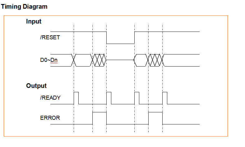
5 | /RESET | Input | TTL, Low level reset to channel 0. High level means channel selection bits are effective. |
6 | /READY | Output | TTL, Ready (High=Not ready, Low=Ready) |
7 | ERROR | Output | TTL, Error (High=Error, Low=No error) |
8 | GND | Input | Ground |
9 | +5VDC | Input | 5.0±5% VDC Power Supply (max 550mA) |
DB-15 male connector (max.1×32)
Pin No. | Signal Name | I / O | Description |
2 | D0 | Input | TTL, Channel selection bit 0 |
3 | D1 | Input | TTL, Channel selection bit 1 |
4 | D2 | Input | TTL, Channel selection bit 2 |
5 | D3 | Input | TTL, Channel selection bit 3 |
6 | D4 | Input | TTL, Channel selection bit 4 |
11 | /RESET | Input | TTL, Low level reset to channel 0. High level means channel selection bits are effective. |
7 | /READY | Output | TTL, Ready (High=Not ready, Low=Ready) |
8 | ERROR | Output | TTL, Error (High=Error, Low=No error) |
1, 9 | GND | Input | Ground |
15 | +5VDC | Input | 5.0±5% VDC Digital power supply (max 50mA) |
12 | VM | Input | 5.0±5% VDC or 12±5% VDC Drive power supply (max 500mA) |
10, 13, 14 | NA |
DB-25 male connector (max.1×128)
Pin No. | Signal Name | I / O | Description | ||
15 | D0 | Input | TTL, Channel selection bit 0 | ||
16 | D1 | Input | TTL, Channel selection bit 1 | ||
17 | D2 | Input | TTL, Channel selection bit 2 | ||
18 | D3 | Input | TTL, Channel selection bit 3 | ||
19 | D4 | Input | TTL, Channel selection bit 4 | ||
20 | D5 | Input | TTL, Channel selection bit 5 | ||
21 | D6 | Input | TTL, Channel selection bit 6 | ||
22 | /RESET | Input | TTL, Low level reset to channel 0. High level means channel selection bits are effective. | ||
2 | /READY | Output | TTL, Ready (High=Not ready, Low=Ready) | ||
3 | ERROR | Output | TTL, Error (High=Error, Low=No error) | ||
1, 10, 14, 23 | GND | Input | Ground | ||
12, 25 | +5VDC | Input | 5.0±5% VDC Digital power supply (max 50mA) | ||
13 | VM | Input | 5.0±5% VDC or 12±5% VDC Drive power supply | N≤45 | Current supply ≤500mA |
11, 24 | N≤88 | Current supply ≤750mA | |||
N≤128 | Current supply ≤1000mA | ||||
4, 5, 6, 7, 8, 9 | NA | ||||
![]() Channel Selection Table
Channel Selection Table
Max Channel | Input | Active Channel | |||||||
/RESET | D6 | D5 | D4 | D3 | D2 | D1 | D0 | ||
N=16 | 0 | x | x | x | x | x | x | x | 0 reset |
1 | x | x | x | 0 | 0 | 0 | 0 | COM → 1 | |
x | x | x | 0 | 0 | 0 | 1 | COM → 2 | ||
x | x | x | 0 | 0 | 1 | 0 | COM → 3 | ||
x | x | x | … | … | … | … | … | ||
x | x | x | 1 | 1 | 1 | 1 | COM → 16 | ||
N=128 | 0 | x | x | x | x | x | x | x | 0 reset |
1 | 0 | 0 | 0 | 0 | 0 | 0 | 0 | COM → 1 | |
0 | 0 | 0 | 0 | 0 | 0 | 1 | COM → 2 | ||
0 | 0 | 0 | 0 | 0 | 1 | 0 | COM → 3 | ||
… | … | … | … | … | … | … | … | ||
1 | 1 | 1 | 1 | 1 | 1 | 1 | COM → 128 | ||

![]()

![]()


